
AI search could not be completed. Please try again or adjust your search.
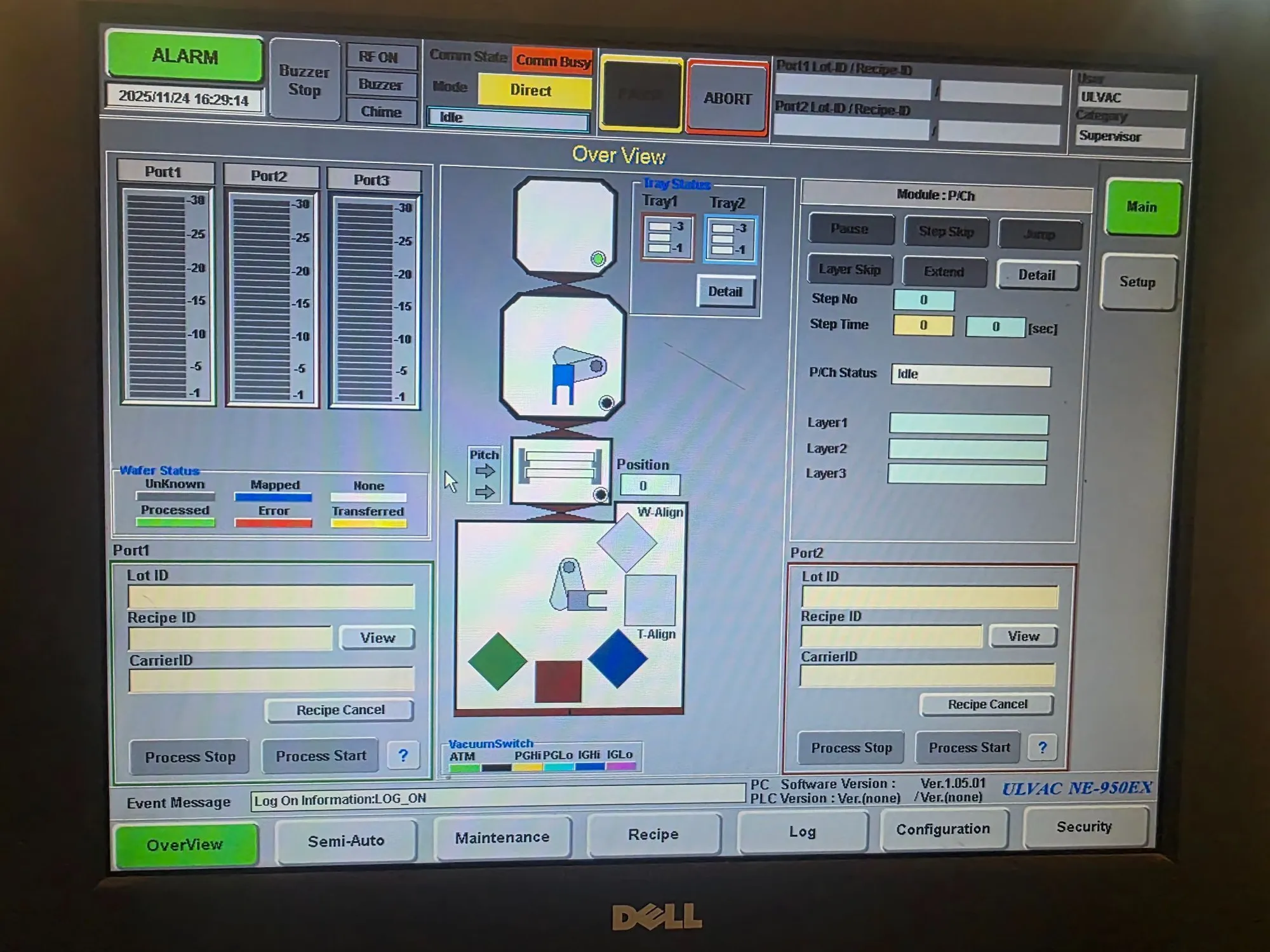
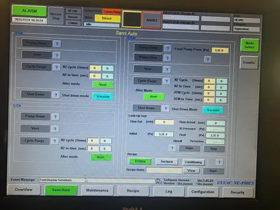
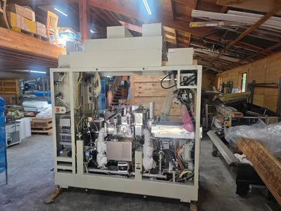
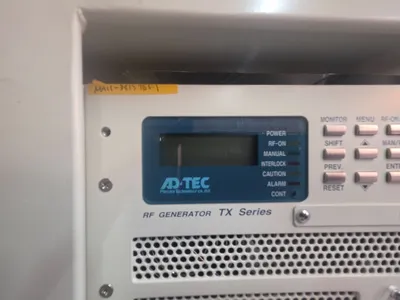
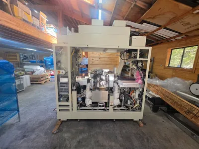
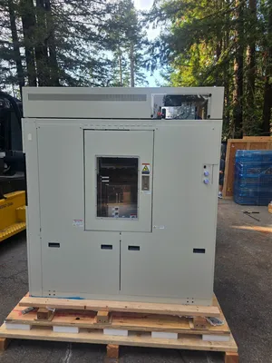
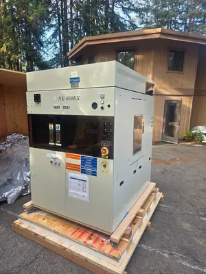
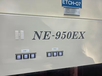
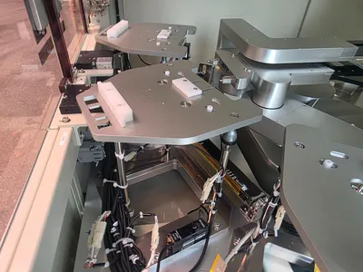
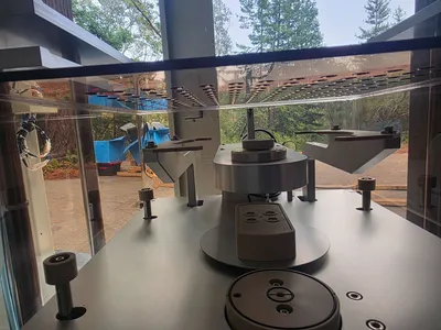
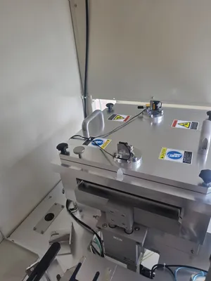
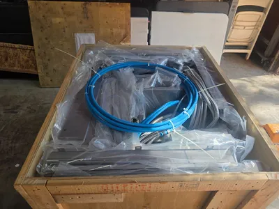
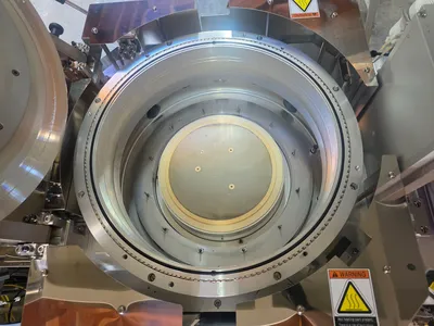
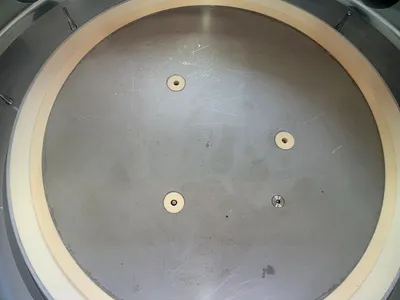
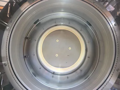
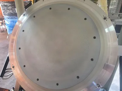
ULVAC NE-950EX ICP / RIE Etch System. (High-Throughput Dry Etcher for Compound Semiconductors / LED / MEMS).
Manufacturer: ULVAC. Model: NE-950EX
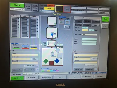
System Type: Inductively Coupled Plasma (ICP) / Reactive Ion Etching (RIE) with magnetic confinement (ISM) — delivers high-density plasma with excellent uniformity and anisotropy. Throughput / Wafer Handling: Batch-type system supporting up to
29 wafers (2″), 12 wafers (3″), 7 wafers (4″), or 3 wafers (6″) per load.
Supported Materials / Applications: Designed for compound-semiconductor and LED manufacturing. Compatible with etching of GaN/AlGaN, sapphire, metals, ITO, SiC, AlN, ZnO, and other III-V or hard materials. Also suitable for MEMS, optical devices, and other thin-film / etch applications.
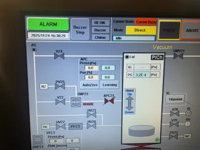
High-density ICP with magnetic confinement (ISM) and proprietary “Star” electrode for uniform plasma distribution and reduced re-deposition.
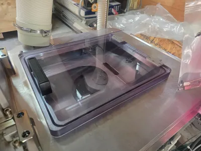
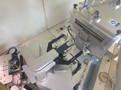
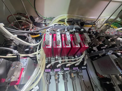
Backside helium cooling and temperature-controlled cathode for wafer thermal management; automated cassette-to-carrier wafer load.
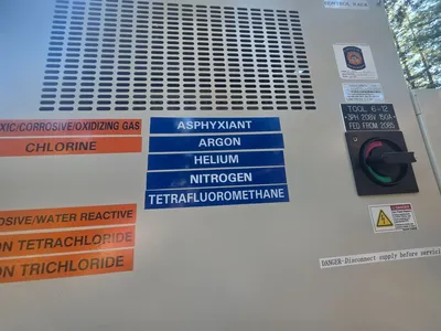
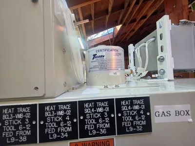
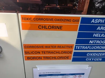
Flexible gas chemistry supporting process gases such as BCl₃, Cl₂, SiCl₄, CF₄, SF₆, C₄F₈, O₂, Ar, enabling both F- and Cl-based etches for metals, semiconductors, dielectrics, etc.
Use Cases: Ideal for high-volume LED manufacturing, compound-semiconductor device fabrication, MEMS, optical device structuring, sapphire or hard-material etching where high plasma density, uniformity, and throughput matter.
Contact us with any questions, or to schedule an inspection or to make shipping arrangements. More images available upon request.
| Dimensions | 100 | 100 |
| Weight | 6000 | 6000 |
ULVAC NE-950EX ICP / RIE Etch System. (High-Throughput Dry Etcher for Compound Semiconductors / LED / MEMS).
Manufacturer: ULVAC. Model: NE-950EX
System Type: Inductively Coupled Plasma (ICP) / Reactive Ion Etching (RIE) with magnetic confinement (ISM) — delivers high-density plasma with excellent uniformity and anisotropy. Throughput / Wafer Handling: Batch-type system supporting up to
29 wafers (2″), 12 wafers (3″), 7 wafers (4″), or 3 wafers (6″) per load.
Supported Materials / Applications: Designed for compound-semiconductor and LED manufacturing. Compatible with etching of GaN/AlGaN, sapphire, metals, ITO, SiC, AlN, ZnO, and other III-V or hard materials. Also suitable for MEMS, optical devices, and other thin-film / etch applications.
High-density ICP with magnetic confinement (ISM) and proprietary “Star” electrode for uniform plasma distribution and reduced re-deposition.
Backside helium cooling and temperature-controlled cathode for wafer thermal management; automated cassette-to-carrier wafer load.
Flexible gas chemistry supporting process gases such as BCl₃, Cl₂, SiCl₄, CF₄, SF₆, C₄F₈, O₂, Ar, enabling both F- and Cl-based etches for metals, semiconductors, dielectrics, etc.
Use Cases: Ideal for high-volume LED manufacturing, compound-semiconductor device fabrication, MEMS, optical device structuring, sapphire or hard-material etching where high plasma density, uniformity, and throughput matter.
Contact us with any questions, or to schedule an inspection or to make shipping arrangements. More images available upon request.